
▼ State of the art
Script to ppt
Free mode
100% free
Freemium
Free Trial
Other tools
-
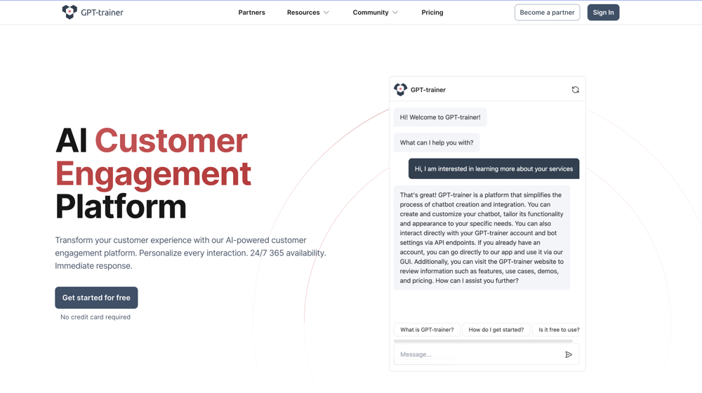 John Griffith🙏 64 karmaJun 16, 2024@GPT TrainerGPT Trainer is run by a highly responsive management team and support staff. Questions are answered quickly, feature requests are incorporated quickly. We have multiple chatbots that are live with GPT Traner, including for Healthcare, hospitality and solar energy providers. We highly recommend for both value and quality.
 -
-
 Great tool! Was very helpful in content production
 -
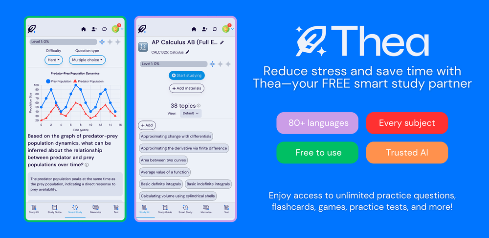 Went from a C to an A in Cognitive Psychology using Thea!!
 - Spotlight: Notis (Personal assistant)
-
 I’ve been using UX sniff for a little while now and I absolutely love it! It’s brilliant! It’s very easy to use, very easy to set up and the support has been spot on. It’s really been helping me with my Business - Pawfection Pet Products. I highly recommend this product.
 -
It's great, I built it and use it daily :)
-
 OpenMeet remio 2.0: Your Personal ChatGPT 1.💡 Personalized Insights, Powered by Your Knowledge Get uniquely tailored AI insights that go beyond generic answers by combining your personal notes and files. 2.🧠 Effortless Memory Capture, No Manual Organizing Automatically indexes all your connected files in real-time, making your entire knowledge base instantly chatable with AI. 3.🎙️ Unlimited Free Recording Transcription Record and transcribe any online or offline conversation, and instantly generate AI summaries with key decisions. 4.🌍 Unified Hub for All Your Data Integrates everything from websites to Slack and emails, creating a single, searchable encyclopedia for all your information. 5.🤖 Your AI Copilot, Everywhere You Work Get instant AI help to summarize, draft, and find answers in your editor or browser without switching apps or breaking your flow. 6.🔒 100% Privacy, 100% Yours With a "Local First" design, all your information is securely stored on your device, keeping your knowledge completely private.
 -
 Define your ideal customers and craft a winning marketing strategy with Elsa.OpenI rarely leave reviews, but Elsa amazed me. After a few weeks of using it, I'm still excited. Props, guys.
 -
 Privacy-first & designed your for mind, and life at workOpenI joined Kin's beta program on my iPhone XR. After upgrading to an iPhone 13, I found that I couldn't log into my existing account on the new phone, forcing me to create a new account. Now, I have two separate Kin accounts on different phones. Today, when I accessed the beta version of Kin, I got a notification stating that the test version ended on Monday, September 23rd. It instructed me to back up my data and move to the official Kin app. I did as advised—backed up my data, confirmed, uninstalled the beta app via TestFlight, and installed the official Kin app. However, when I attempted to “log in”, I was still unable to access my existing account. This issue hasn't been resolved yet. I have been trying desperately to get in contact with the support team. I left feedback through the test flight app and sent emails. No response. Now trying to find a forums, Reddit posts, TAAFT comments☻
 -
6 seconds of video generation per month for free accounts
-
Very cool app! Build was fast as, and with a few tweaks I fully launched my website in 1 hour!
-
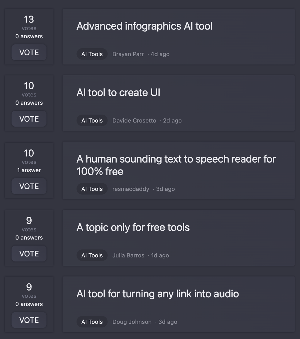
- Didn't find the AI you were looking for?
-
 Enterprise-grade open-source AI inference at unlimited scale.Open
 -
I've been playing around with this for a few hours. It's made me say "WOW" too many times than i wish to admit. I'm going to follow this and see how it evolves. For now, i managed to create quite a nice Expenses app for personal use. | It did have some problems when it came to moving some components on other pages, but for how short the prompts it uses can be, it is really impressive. With some proper prompts it can generate some strong stuff.
-
This is not the case. You can create both a blog and a podcast with the free account. We have a support link, please use that and I would be happy to walk you through this if the videos did not help.
-
 Open
Open -
-
Hi Rod, you did not click the "include" for each section you wanted to include. I did that for you so you can now see your page. Looks good so far.
-
WhatsApp and Messenger integrations don't work very well. Support team is very sporadic. Still couldn't get it to work consistently despite best effort to fix.
-
All I can say is WoW! I don't know too terribly much about Tarot, but my reading was 110% spot on. And I am not referring only to the fact of the cards drawn couldn't have come closer if I hand-picked them but it was the analysis of each card individually, as well as overall. I'll be using this regularly from now on.
-
-
Amazing tool for beginner investors. Just enter your investment amount, risk tolerance, investment goal, investment timeframe, and get a portfolio in seconds.
-
 100% Free AI-powered website compliance audits in minutes.OpenUsed this tool to fix my compliance issues in a day.
 -
Base44: The all-new builder A new era of Base44 where creating apps is smarter, faster, and more intuitive. The all-new builder doesn’t just code, it thinks: “What do I need to create this app?” and knows how to make it happen — through web search, smart file search, log inspection and data fetching. App building that understands context. Intelligence meets creation.
-
Much more in-depth and relevant outputs from my existing chatGPT from the first interaction.
-
Stakly helped me launch my app super fast. Really impressed with how easy it was to use.
-
 Ellie, your AI for crafting personalized email replies.Open
 -
Purely magic. It increases the productivity by a lot and the process is pretty addictive. I've been building websites like there's not tomorrow.
-
-
 AI-powered prediction market picks delivered weekly for $10/monthOpen
 -
My favourite AI application. Great clean UI and even better pricing.
-
-
Super easy to use and completely open source.
-
Thanks for all the feedback on our last release — the one where we introduced one-click product import, story-driven videos, automated templates, brand vault, and smarter AI characters. This week’s update focuses on making those features smoother, more reliable, and more polished across all product types. Latest Updates - Translated pages now work more smoothly. - Spokesperson videos now come with matching B-rolls. - Digital products now use a new benefits-focused style. - Physical products now require a product image for better video quality. - Other bug fixes and improvements
-
 Turn your ideas into stunning, custom phone cases - instantly, with AI.Open
 -
This is awesome. It tells me the answers to my practice exam questions automatically through my airpods without me having to do anything, just by seeing my exam through my phone camera. I've been looking for an AI tool like this for a while.
-
-
 OpenI built Remy to solve a problem I face every day: Newsletter overload 📬 Remy is your personal AI assistant that summarizes all your newsletters into a single digest email. Go from a cluttered inbox to a clear, concise briefing in one go.
 -
-
Amazing deep research feature! Haven't seen this level of execution through any other tool. It gives a designed socket to view a presentation at the end.
-
 SCORM-compliant, Interactive course builder, personalized learning, tools instructional designers, Teacher toolsOpenI’ve been using Mexty for a few weeks now and it honestly makes lesson creation so much easier. The interface is clean, and I can build interactive content in minutes without needing to code. It’s been super helpful for saving time and still getting professional results.
 -
-
The leading generative media models on fal combined with top-earning real-world creative talent on Contra is a powerful combination. Feedback to fuel the future of creative ai.
-
-
Hey TAAFT 👋 I'm Vincent, the founder of BlogSEO. I created BlogSEO with one goal in mind: automating SEO for busy entrepreneurs. As a multiple-time founder myself, I never had the time to take care of SEO for my past projects. I knew SEO was one of the most efficient acquisition channel, but I just couldn't spend time creating content and setting up a blog for my projects. I was busy building the features, answering customers and running the business. That's why I created BlogSEO. For ambitious builders and business owners that know the power of ranking on Google and getting cited by ChatGPT to get leads, but don't have the time to take care of it. BlogSEO fully automates your SEO strategy: you just need to put your website URL, connect it in a few clicks and fresh SEO-friendly content will start appearing on your website daily. BlogSEO was designed to really work for you and not the other way around, that's why it works out of the box with 0 setup and is fully automated by default. But if you prefer to have more control over your content, you're able to do so by customizing keywords, targeting competitors and review the SEO content before it's published. I hope this tool will help you as much as it helps me getting organic traffic on my websites! Keep Scaling 🚀! Vincent
-
 Your Visitors Can Talk to Your Website. AI Answers Instantly.Open
 -
 Create AI assistants that chat, talk, and answer from your data.OpenHi there, I’m Alix, co-founder of Invent. We’re building the future of Customer Support UX, where humans and AI truly collaborate. Would love to read&hear your thoughts. DM for any questions. We ship fast!
 -
 Turn everyday items into enriching learning experiences.Opentried this tool and while it wants you to sign up at some point, it does provide some good options whenever you run out of ideas, definitely recommend it
 -
Hi! I'm Regitze, founder of Digibate - your AI-powered marketing assistant built especially for small businesses and solopreneurs. We help you create, schedule, and publish content effortlessly across platforms, including product photoshoots, social posts, newsletters, and more. We're constantly working on improving Digibate, and your feedback means the world to us. If you have any thoughts, ideas, or wishes for future features, please don’t hesitate to share - we’d love to hear from you! 💡
-
It’s a fast, sleek, and feature-rich browser that makes multitasking effortless and browsing more enjoyable. Highly recommended!
-
the founder is cool, definitely a recommendation if you have personal requests and grow the app along with you.
-
Like copilot, but for power users. Nice for my n8n workflows command center
-
This is without doubt, the fastest and easiest way to compare and test different AI models side by side
-
-
 Open
Open -
Made writing my first book simple and fast. I turned scattered ideas into a full, professional manuscript in a weekend. The guided flow kept me focused, and the editing felt natural.
-
 Instantly translate manga into 100+ languages with AI.OpenThis tool supports real-time comic translation on many websites, and can also support cross-platform progress synchronization of about 10 websites, which is very convenient!
 -
I’m allergic to synthetic data, but I gave FirstSign a spin and… my calendar sent a thank-you note. Skipped the cold DMs and got surprisingly sharp interviews for early validation. Feels like cheating, but I’ll allow it ;)
-
 Prevent AI data breaches with real-time risk management.OpenNot just alerts - real time visibility for Slack, Google Workspace, and AI APIs to stop risks before they become breaches
 -
Thanks for the feedback! Would love to hear what you’d like to see next
-
-
Great tool for engaging customers and repurposing content! I also made a video on it https://youtu.be/cIEUz3bxPRc
-
It's a powerful AI-powered personal knowledge system that brings together links, files, notes, and documents in one unified workspace. It's like Notion meets Raindrop meets Google Drive, but with an AI layer that helps you resurface forgotten content, cluster related topics, and even draft documents based on your saved materials.
-
 Open👋 Karl, Co-founder here. We built IRL PLAYground because we believe a child’s first contact with AI should be ethical, creative, and human-centered. Not a tool that replaces their teachers and play environments, but one that works alongside them to unlock imagination and the potential of learning spaces. This first release focuses on the invisible work teachers carry: lesson planning, materials, classroom flow. Not flashy, but foundational. We didn’t build an MVP. We built the infrastructure of play. And this is just the start. It’s designed to be in classrooms now, and soon we’ll bring it into the home. If you’re a teacher or parent, we’d love your feedback, all ideas welcome. Share to those that need it, and let’s build this together.
 -
-
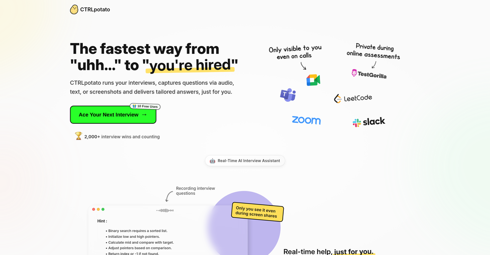
 Turn interview anxiety into confidence with AI-powered practice and real-time feedback.OpenNice concept.. If the AI can actually simulate realistic interviews, this could be super useful.
 -
Hello everyone, As a AI power user, I constantly faced the multi-tab scramble and the uncertainty of getting truly reliable answers from various AI tools. That frustration led me to build Singulairity AI. My goal was simple: to create a unified, intelligent, and trustworthy platform where you can access leading AI models with unprecedented clarity and efficiency. I poured my efforts into features like Intelligent Auto-Routing, Side-by-Side Response Comparison, and the innovative Truth Mode to give you the confidence I always sought. I truly hope Singulairity AI enhances your workflow. Please review the tool and share your invaluable feedback; it's essential for Singulairity's continued evolution.
-
look nice! I still explore more on this platform, and this tool is the first and the best one I have even used!
-
I’ve been using Lyra as a kind of MBA writing coach—it helps structure ideas, spot what’s working in your story, and take the pressure off the blank page. Your voice is still doing the work; this just gives it a bit more shape.
-
 Your AI stream companion that entertains chat and boosts tipsOpeninteresting tool, thank you
 -
AgentFuel.bot auto-generates social media content specifically for the real estate industry, has a document chat tool and the road map is super strong. If you are a commercial or residential real estate agent, mortgage loan officer or in title, anywhere in the world this tool is worth a look.
-
Hey, wonderful TAAFTers! We made outwrite.ai to quickly generate articles, blogs, and posts that are structured in the EXACT format that AIs prefer to find, scan, and include your brand when buyers are asking questions about your category. You become part of THE answer AI gives. Most brands still create content for Google's algorithm: keywords, backlinks, LOTS of money, and...hope. AI search doesn't work the same way as Google. When someone asks ChatGPT, Gemini, or Perplexity for a product recommendation, the AI produces a single answer. If your brand isn't in that answer...you're invisible. That's the challenge outwrite.ai solves: LLM citation optimization. Now, page 10 brands can get cited along with Fortune 500 market leaders...without a penny spent on ads.
-
-
The models here really help w/ finding investment properties.
-
Hey this is Tan, I'm the creator of NotesBot. I created this tool because I needed it for my own meetings. After using myself and getting great summarization reviews from my peers, I decided to release it to the public. After release, we realized people were also using it for Dungeons and Dragons, I then added a DnD mode. This tool is non-invasive, very easy to set up, and perfect for meetings. I hope you enjoy using it!
-
Cool concept (coming someone that is bad at texting). I like how simple it is and how it breaks down the convo into clear insights (who texts more, response times, and crush score).
-
 OpenMagnetify's clean and simple interface makes it incredibly easy to jump in and start creating marketing materials. The lead magnet templates are a total game-changer for creating lead magnets to grow our list. Magnetify has already become an essential tool for our marketing strategy!
 -
Hey TAAFT! 👋 I'm Advait from OpenGradient, and we're thrilled to launch MemSync - a unified memory layer for all your AI apps. Why we built this: Like many of you, we were frustrated by AI's amnesia problem. Every time we switched between ChatGPT, Claude, or Perplexity, we had to start from scratch - re-explaining our context, preferences, and ongoing projects. The most advanced AI models in the world couldn't remember a conversation from yesterday. What's unique about MemSync: - Universal compatibility: One extension that works across ALL major AI platforms - not locked to a single tool - Intelligent context sync: Your conversations flow seamlessly between different AI models - Privacy-first architecture: End-to-end encryption ensures your memories stay yours - Zero setup friction: Install once, and every AI tool instantly remembers you What we're most proud of: The simplicity. While others are building complex integrations, we focused on making memory "just work." Users tell us it feels magical when Claude picks up exactly where ChatGPT left off. One founder said it's "like giving AI a shared notebook about me that actually persists." We've been quietly testing with a small group, and the feedback has been incredible - people save 15-30 minutes daily just from eliminating repetitive context-setting. Today's launch includes our Chrome extension with support for ChatGPT, Claude, Grok, and more coming soon. Relevant Links: • Website: https://www.memsync.ai/ • Github: Open-source soon!
-
We’ve just launched CASi Scout — a product that helps writers generate smart, relevant content ideas based on breaking news, strategic angles, and their client’s audience and product.
-
 Open
Open -
As someone who's worked with food businesses, I know how crucial visual appeal is for driving sales - especially in the digital space where customers make split-second decisions based on photos. What stands out to me is how this tool addresses a real pain point. Professional food photography is expensive and time-consuming, but this AI solution makes high-quality food images accessible to everyone from small restaurants to food bloggers. The instant transformation aspect is particularly valuable for businesses that need to update their menus frequently or manage multiple locations. I can see this being a game-changer for food delivery apps where compelling visuals directly impact order volume. The fact that it's specifically trained for food photography rather than being a generic photo enhancer shows thoughtful development. Would love to see some before/after examples if the developers are sharing any - the concept is solid and fills a clear market need. Definitely keeping this on my radar for future projects!
-
 Generate professional AI dating photos for 3x more matches.OpenHey, I'm Jacob. Indie developer, built a few AI products. My friend complained about no matches on Tinder. His photos were terrible - bad lighting, messy backgrounds, awkward angles. "Get better photos." "Photographers are expensive and it's weird doing a photoshoot for dating apps." He was right. What I built Spent 2 weeks building this with Stable Diffusion and Claude. Upload 10-15 photos, generates 80-180 dating photos in ~20 minutes. The tricky part: making them look real, not AI-generated. Most AI headshot tools optimize for LinkedIn. Dating photos need to feel natural. Optimized specifically for Tinder, Bumble & Hinge - each platform has different vibes. Added a "realness score" to filter out obvious AI stuff. Current issues - Hands are still weird sometimes - Some photos don't quite look like you - Background inconsistencies Tested with ~40 people. Most said it helped. Some photos were off. Why I'm posting Not sure if this is actually useful or just solving my friend's specific problem. If people care, I'll keep improving it. If not, learned a lot anyway. Link: https://datephotos.ai/
 -
It greatly supported my R&D work by helping me tackle technical challenges and prepare reports.
-
Recently released an AI Chat Bot for websites and was testing different models for my ”conversion-focused” approach, this would have made it so much easier! Could be interesting to be able to plug into this via API with all my data
-
-
Hello Everyone, My name is Mohamed, the Co-Founder of linesNcircles.com. At linesNcircles our mission is to revolutionize AI & Humen Interaction. Our first product TheBar is an AI agent which can build websites for you, edit them, saves files locally, browses the internet and provide you with answers to your questions all in very simple interface. TheBar runs on your computer without signup. Your website files are saved locally with the option to publish them under our website with one click. All your files are under your creations folders. We built TheBar to be simple to use, super fast in building things for you and we are working tirelessly, to bring in more features for you like writing pdf documents and making presentations which are coming soon. Check TheBar out it is available for free now on our website https://www.linesncircles.com. We would love to hear your feedback and comments
-
Hi folks - I'm Charles, the founder of Wizardly. As a sales guy I originally built this app to create training videos for sales reps 10X faster. Many friends started using Wizardly to create all sorts of tutorials for tools I'd never heard of. Excited to get feedback and hear how I can make this app the best how-to video generator on the market.
-
I gain time with TopFrog! It is very helpful, and I recommend it highly!
-
 Build customized Proof-of-Concepts (POCs) and full applications in hours - not weeks.Open
 -
-
This its best AI bot i have used, its very quick and accurate, nice experience, its like im talking to real human with all emotions
-
Ahaha Sam was really nice to me, we did some brainstorming together. It s great for getting some strategies ideas, especially if you have a small business like me
-
Incredibly easy way to connect to Amazon products and pull information
-
tried this tool on a random photo and it hit quick. gave me three likely matches with percents and simple care tips so i actually learned something. free and cute app
-
Hey everyone! It's Noel, cofounder of Tinkery. We launched recently, growing rapidly and always welcoming feedback to continue improving the platform. Please reach out!
-
Hey! Thanks for your interest — we’ve opened up applications for the Early Access Program of our AI Agent for Mobility and Logistics. You can apply here: https://getswitch.io/agentic-ai-for-mobility-and-logistics/
-
Protaige really made my life easier in creating Campaign across different platforms in a single click just by providing my Briefs. Thank you! Awesome Time Saving AI Tool. Really loved using it.
-
I use Olostep to gather data from millions of e-commerce pages for my AI shopping assistant service and it's the most cost-effective and reliable product on the market
-
I would call it a "documentation generator for MCP". Would be great to see support for LM Studio too. Other than that, it looks like this tool already follows the best practices for MCP docs. For example, here is a demo for web scraping with Tavily: https://mcpshowcase.com/p/mcp-server-directory/tavily-mcp-server The docs on how to connect your MCP to different AI assistants are essential, but also a pain to maintain on your own. Also nice to see the auto-generated use cases and sample chats!
-
Super helpful tool! Saved me hours reading comments and gave great insights. Highly recommend for YouTubers!
-
Love the app. Used it to find a good balance in performance to play at a higher graphics setting but with over 100 FPS which was really useful in making Marvel Rivals more enjoyable to play this season!
-
 Assign Jira tickets directly to Cursor agents and get PRs and Previews.Open
 -
 AI agent for Jupyter: Generate code, run cells with natural language.Open
 -
threw it at our dusty help center and it cooked. pulled context from tickets and updates and wrote clean articles and faqs. inbox got quieter fast. solid tool.
-
Been looking forever to find an app like this! Reviews supplement and provides helpful information to optimize your health
-
We’ve been working closely with early beta partners (from startups to global brands) to shape Clamor, and today’s launch is a huge milestone for us. Would love your thoughts, feedback, and honest takes as your input will help us make Clamor even better! What’s the one type of cultural or community insight you wish you had at your fingertips?
-
As the founder of BuildOrNot.io, I’m excited to announce that our platform has just been launched. At this early stage, our most valuable asset is your feedback. I warmly invite you to try BuildOrNot.io and share your thoughts—both the strengths you find useful and the shortcomings we should improve. Your ratings and comments will directly help us refine the tool, enhance the user experience, and make the platform more valuable for every entrepreneur. Your voice matters, and I truly appreciate your support on this journey.
-
 Open
Open -
Realistic couple photo merge and creative generation!
-
 Grotto Slice – Your Shortcut from Image to KlaviyoOpen
 -
 OpenThe tool worked really well for us. It was easy to upload our first PDFs and set up an automated flow through the API
 -
Hi everyone! I’m part of the team behind Sidewalk Social. 👋 We built this tool to help local businesses stop stressing over Instagram and get back to running their shops. Seeing so many of you checking us out here is amazing! I’m hanging out in the comments today, so if you have any questions about how the automation works, feel free to ask. If you’ve had a chance to test it out, we’d be incredibly specific for your honest rating or feedback. It really helps us improve! Cheers!
-
AskNova Dream Interpretation helps people reconnect with their dreams in a more vivid and meaningful way. Instead of just typing out what you remember, the experience combines immersive soundscapes and guided prompts to bring back the feelings and details of your dream, making recall easier and deeper. It’s an AI-powered tool that is designed to feel more like a journey of self-reflection rather than a simple analysis.
-
Had an incredibly insightful meeting with the team. It’s definitely worth your attention if you’re planning to automate your property management.
-
I have used cheers to review several different companies around me and it has been a much better experience than traditional methods like QR codes. I love seeing cheers when I try out new businesses.
-
Hey Thanks for the insightful review. You have raised some important points. It is $9/month and we do have a trial now and adding more options.
-
 Never miss another customer with 24/7 AI Voice Assistants. No code setup.Open
 -
Easy and efficient tool, I like the carousel generator
-
-
 Slash Your Tech Stack Costs by 40-50%. Helping SMBs save $$$Open
 -
Just tried the tool and printed my first 3D model, and I’m honestly surprised by how good it came out. It was super easy to use, and the final print matched my reference image perfectly. Congrats to the Mimetic Labs team for building such a simple but super cool tool.
-
I am a SRED consultant. The ability to upload documents and instantly get SR
-
Really love using PR.co. Super easy to set up and our team can share press stuff way faster now. It saves us a ton of time and just makes the whole PR job less stressful.
-
 Create digital vCards and WhatsApp shops in minutes.Open
 -
-
 All-in-one AI kitchen assistant: pantry management, recipe generation, meal planning, shopping listsOpenThis app is great- I use it weekly to create meal plans, recipes, and reduce waste and save money by using leftover ingredients that I already have!


Ask the community

Hoang Frank
Mar 3, 2025
Slide 1: Title Slide
Title: "Understanding Probe Cards: History, Structure, Principle, and Value"
Subtitle: A Comprehensive Training Guide
Details:Presented by [Your Name], Date: March 2, 2025
Visual: Image of a probe card or semiconductor wafer
Notes: Keep it clean and professional; use a tech-themed background.
Slide 2: Agenda
Title: "What We’ll Cover Today"
Text:
Introduction to Probe Cards
History of Probe Cards
Structure of Probe Cards
Working Principle
Value in Semiconductor Industry
Visual: Simple numbered list or icons for each topic
Notes: Set expectations for the audience.
Slide 3: What is a Probe Card?
Title: "Probe Card: The Basics"
Text:
An interface between test equipment and semiconductor wafers.
Used in automated integrated circuit (IC) testing.
Ensures electrical validation before dicing and packaging.
Visual: Diagram of a probe card connecting a tester to a wafer
Notes: Emphasize its role as a critical testing tool.
Slide 4: Why Probe Cards Matter
Title: "Importance in Semiconductor Manufacturing"
Text:
Identifies defects early, reducing waste.
Enables high-volume testing of ICs.
Supports the production of reliable electronics.
Visual: Image of a semiconductor production line
Notes: Highlight cost savings and quality control.
Slide 5: History – Early Beginnings
Title: "History of Probe Cards: The Early Days"
Text:
1960s: Emergence with basic needle-type probes.
Used for simple IC testing during the rise of semiconductors.
Limited to low pin counts and manual processes.
Visual: Vintage photo of early semiconductor testing
Notes: Set the stage for technological evolution.
Slide 6: History – Evolution in the 1980s
Title: "1980s: Advancements in Probe Technology"
Text:
Introduction of epoxy and blade probe cards.
Improved pin density for complex circuits.
Shift toward automated testing systems.
Visual: Image of an epoxy probe card
Notes: Mention the growth of the electronics industry.
Slide 7: History – MEMS Revolution
Title: "1990s–2000s: The MEMS Era"
Text:
Micro-Electro-Mechanical Systems (MEMS) probe cards introduced.
Enabled testing of smaller, denser ICs.
Supported the rise of mobile and computing technologies.
Visual: Close-up of a MEMS probe card
Notes: Highlight precision and scalability.
Slide 8: History – Modern Developments
Title: "Today: Cutting-Edge Probe Cards"
Text:
Full-wafer testing (e.g., 12-inch wafers in one touchdown).
High-frequency and high-pin-count capabilities.
Ongoing innovation for AI, 5G, and beyond.
Visual: Modern probe card in a cleanroom
Notes: Tie to current tech trends.
Slide 9: Structure – Overview
Title: "Structure of a Probe Card"
Text:
Three main components:
Printed Circuit Board (PCB)
Substrate
Contact Elements (Probes/Needles)
Visual: Labeled diagram of a probe card
Notes: Prepare to dive deeper into each part.
Slide 10: Structure – Printed Circuit Board (PCB)
Title: "The PCB Backbone"
Text:
Provides structural support and electrical pathways.
Materials: FR4, ceramic, or advanced composites.
Connects to the tester via edge contacts.
Visual: Image of a probe card PCB
Notes: Explain its role in signal transmission.
Slide 11: Structure – Substrate
Title: "The Substrate Layer"
Text:
Acts as an intermediary between PCB and probes.
Often made of ceramic or silicon.
Ensures precise alignment and stability.
Visual: Cross-section showing substrate placement
Notes: Highlight its mechanical importance.
Slide 12: Structure – Contact Elements
Title: "Probes: The Heart of the Card"
Text:
Needles or pins that contact the wafer.
Types: Needle, Vertical, MEMS.
Pitch: Microns apart for precision.
Visual: Magnified image of probe tips
Notes: Emphasize variety and precision.
Slide 13: Principle – How It Works
Title: "Working Principle of Probe Cards"
Text:
Connects tester to wafer via probes.
Sends electrical signals (test patterns).
Measures responses to validate IC functionality.
Visual: Flowchart (Tester → Probe Card → Wafer)
Notes: Keep it simple and clear.
Slide 14: Principle – Testing Process
Title: "The Testing Workflow"
Text:
Align probe card with wafer (optical alignment).
Probes touch IC pads or bumps.
Tester evaluates pass/fail.
Visual: Animation or step-by-step diagram
Notes: Show the precision required.
Slide 15: Principle – Key Parameters
Title: "Critical Performance Factors"
Text:
Contact resistance: Low for accurate readings.
Pin count: High for parallel testing.
Frequency: Supports high-speed ICs.
Visual: Graph comparing parameters
Notes: Tie to real-world applications.
Slide 16: Value – Cost Efficiency
Title: "Value: Saving Time and Money"
Text:
Early defect detection reduces downstream costs.
High-throughput testing speeds production.
Reusable with proper maintenance.
Visual: Cost-benefit chart
Notes: Quantify savings if possible.
Slide 17: Value – Quality Assurance
Title: "Value: Ensuring Reliability"
Text:
Validates IC performance before packaging.
Critical for high-stakes applications (e.g., automotive, medical).
Reduces field failures.
Visual: Image of a reliable IC in use
Notes: Emphasize trust in tech.
Slide 18: Value – Technological Enablement
Title: "Value: Driving Innovation"
Text:
Supports testing of advanced chips (AI, 5G, quantum).
Adapts to shrinking geometries and 3D packaging.
Fuels the digital revolution.
Visual: Futuristic tech (e.g., AI chip)
Notes: Look forward to future trends.
Slide 19: Challenges and Future
Title: "Looking Ahead"
Text:
Challenges: Tip contamination, wear, cost of customization.
Future: Self-cleaning probes, AI-driven testing, full automation.
Visual: Concept art of future probe tech
Notes: End on an optimistic note.
Slide 20: Conclusion
Title: "Key Takeaways"
Text:
Probe cards are vital to semiconductor testing.
Evolved from simple needles to advanced MEMS.
Deliver cost, quality, and innovation benefits.
Questions?
Visual: Recap image or thank-you note
Notes: Invite discussion and feedback.
Post